
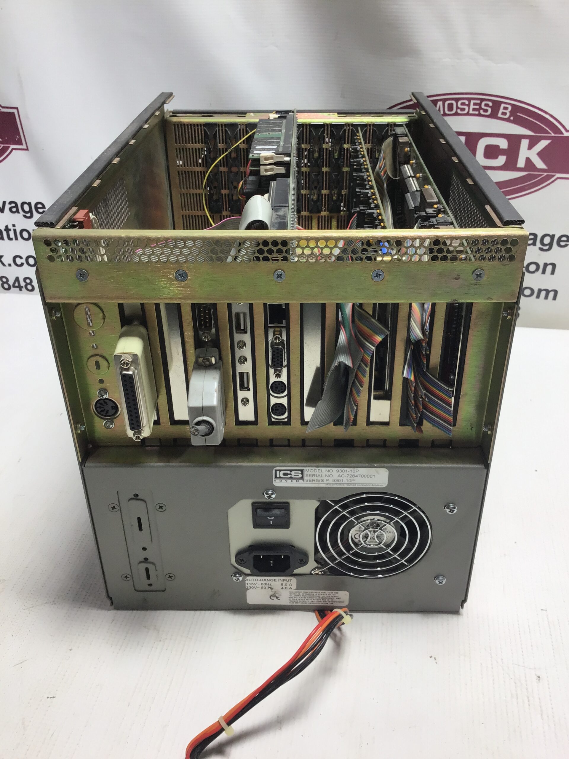
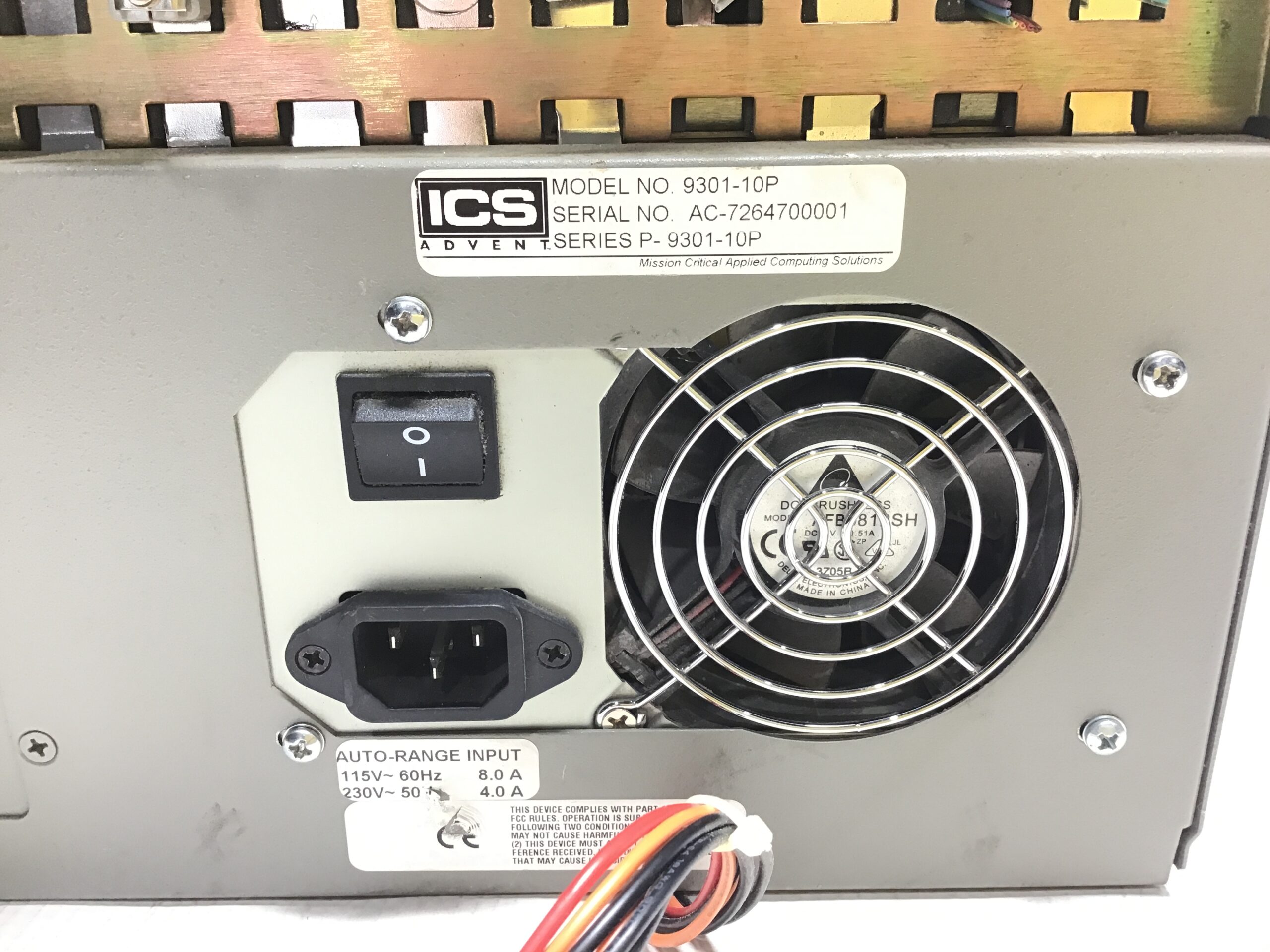
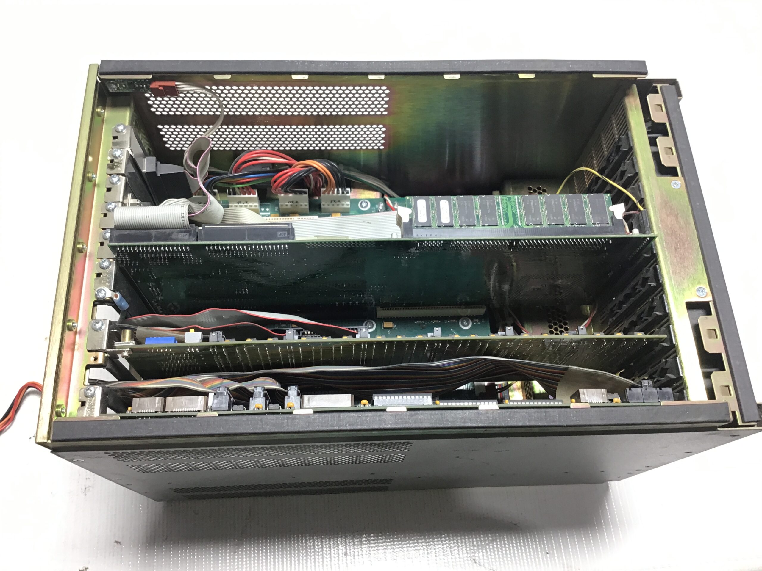
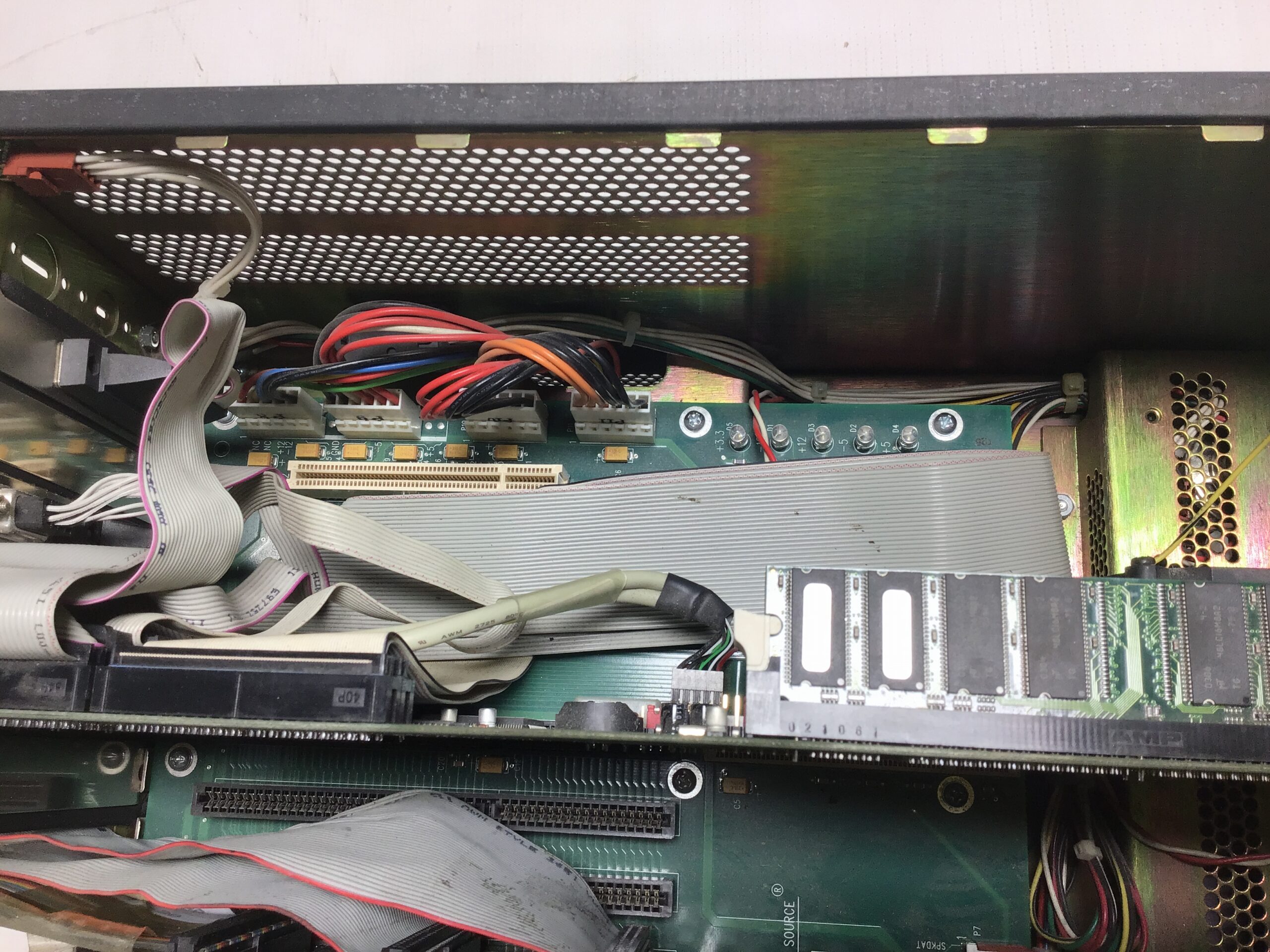
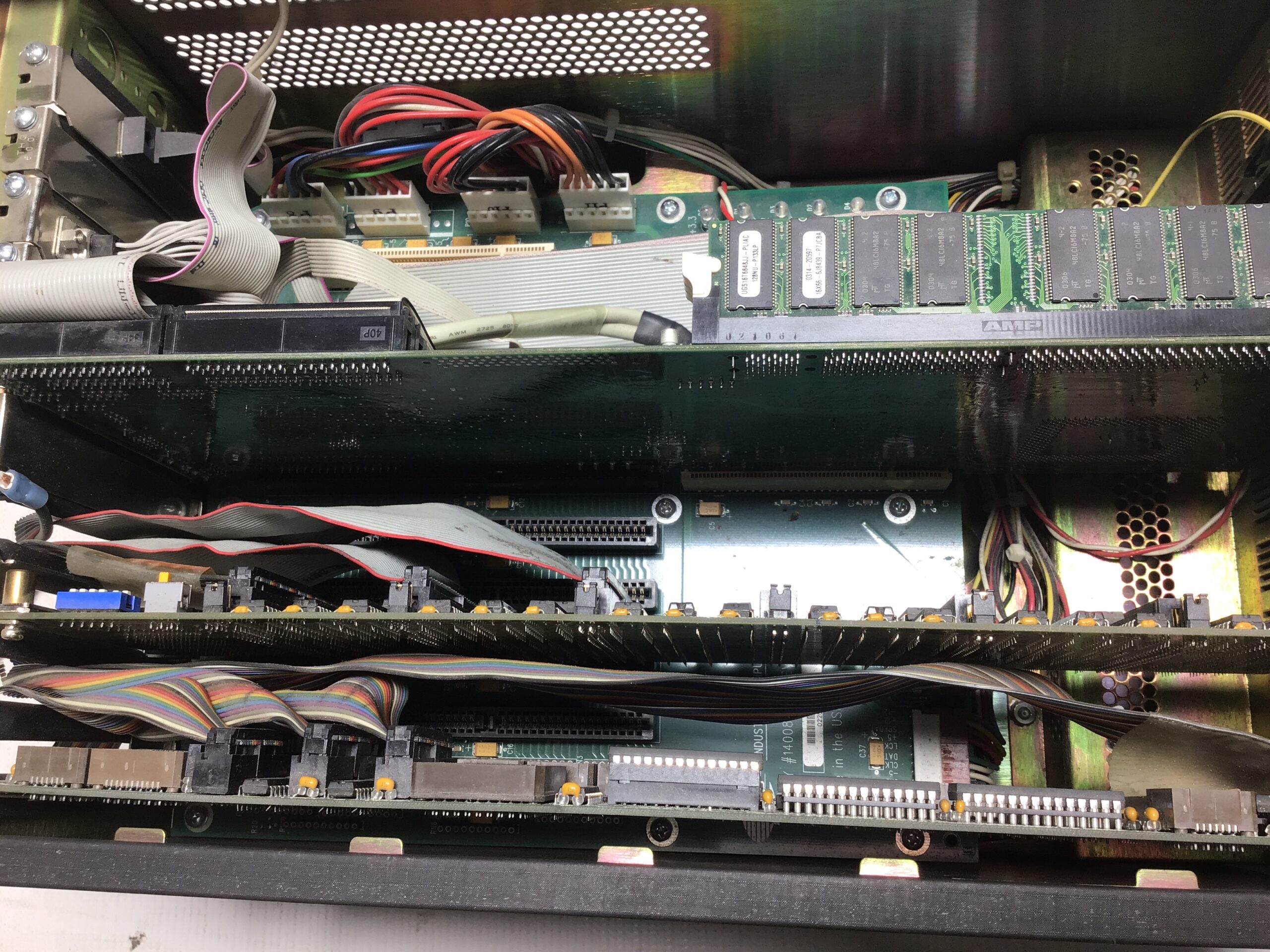
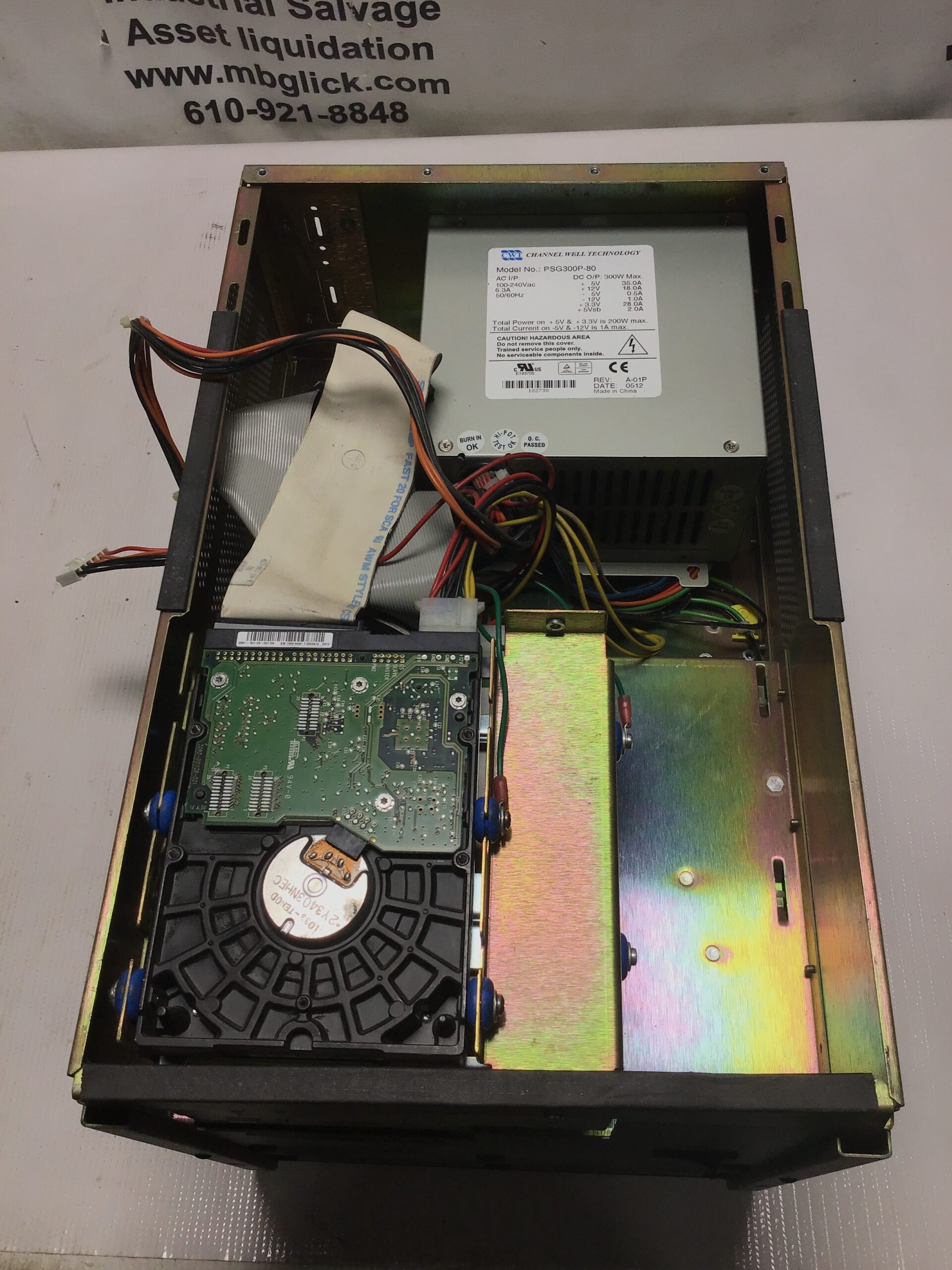
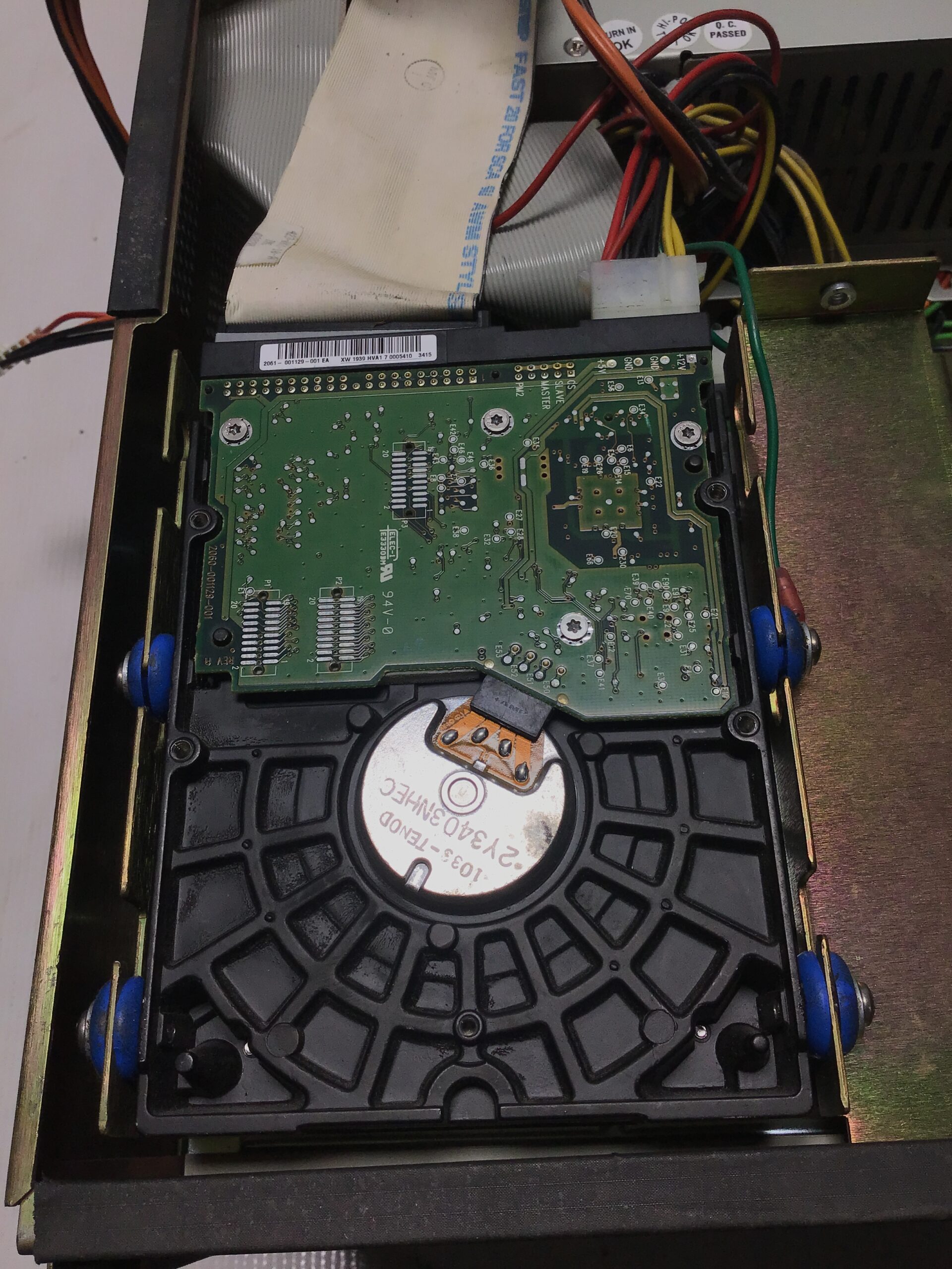
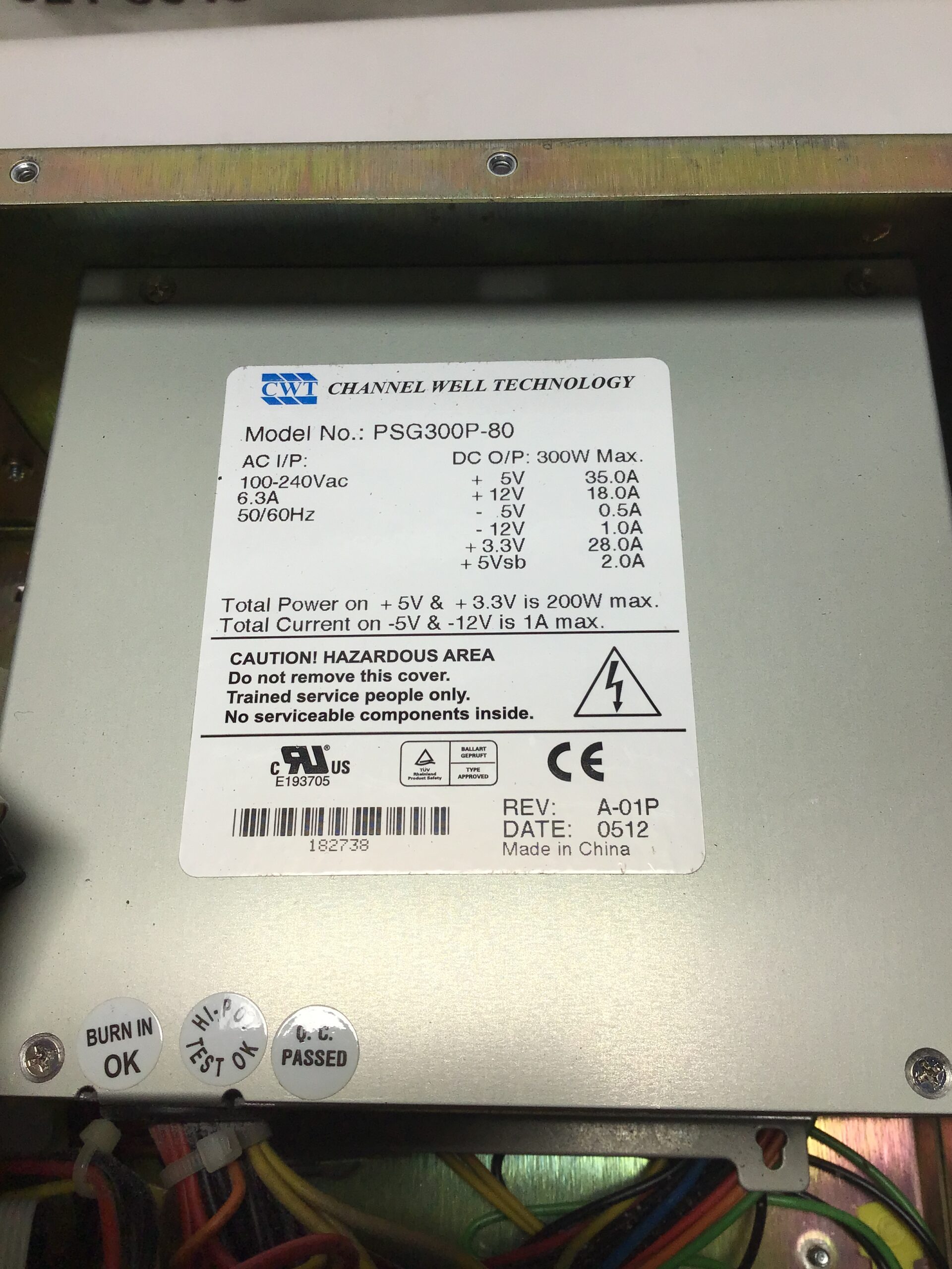
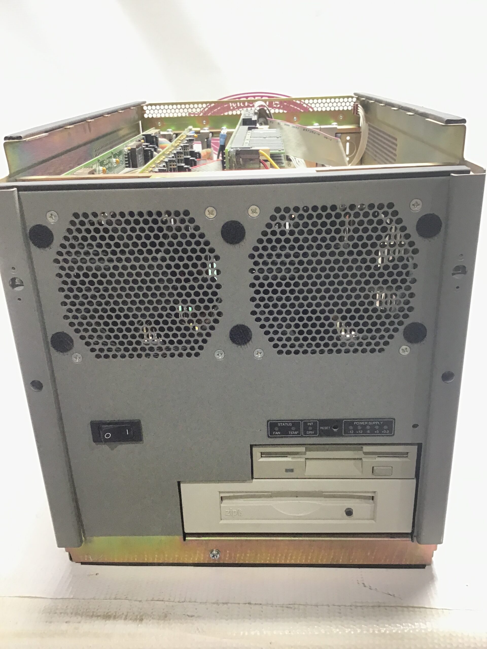
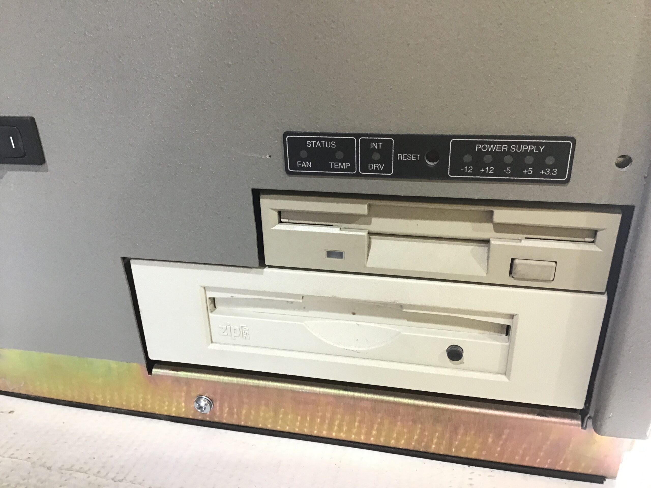
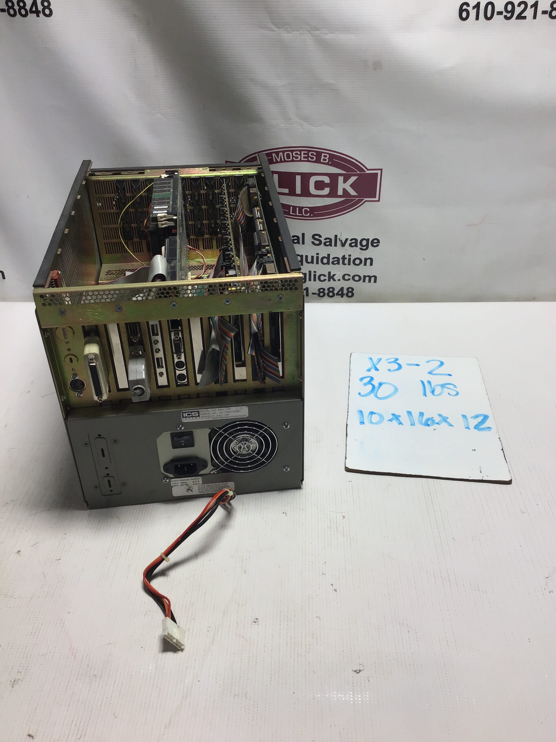
Introducing the ICS 9301-10P Patterned Wafer Defect Tool, engineered for precision and efficiency in semiconductor manufacturing. This advanced tool features an auto range input of 115/230V and operates seamlessly at 50/60Hz, drawing 8.0A or 4.0A depending on the voltage. Its innovative design allows for quick detection and analysis of wafer defects, ensuring high-quality production standards. Enhance your workflow and minimize downtime with this reliable and versatile tool, perfect for any high-tech facility looking to maintain excellence in their processes.
🔬 Precision Wafer Defect Analysis
✔ Designed to detect and analyze patterned wafer defects with high accuracy, supporting semiconductor and microelectronics applications.
⚡ Auto Range Input
✔ Flexible power input of 115/230V, 50/60Hz, operating at 8.0/4.0A, ensuring compatibility with a wide range of lab and facility setups.
🏭 Industrial-Grade Reliability
✔ Built to withstand rigorous use in manufacturing, testing, and research environments.
📊 Consistent Performance
✔ Provides stable and reliable measurements to maintain quality control and improve production yields.
🔄 Versatile Application
✔ Ideal for semiconductor fabrication plants, research labs, and precision testing facilities.
🛠️ Durable Construction
✔ Manufactured with high-quality components to ensure long service life and reduced maintenance needs.

Reviews
There are no reviews yet.